Loading
Showing posts with label Innovations. Show all posts

3-D Projection Tech Makes Images Hover in Mid-Air, No Screen Necessary


Aerial 3D by Burton Using lasers to excite nitrogen and oxygen in the air, the Aerial 3D system produces natural 3-D images in space without using a screen.
It’s a kind of validation when our past visions of the future and the present collide, reminding us that things we thought were possible back then actually were within reach. Take, for example, Tokyo-based Burton’s Aerial 3D technology. The company claims it’s the first 3-D tech that casts three-dimensional objects in mid-air without using any kind of screen. 
Rather than using a screen to generate the illusion of three dimensions, Aerial 3D is a laser system that uses beams of light projected from below to generate plasma excitation in atoms of oxygen and nitrogen in the air. It currently can create 50,000 points of light per second, giving it a somewhat choppy frame rate of 10-15 fps. Burton is working to improve that to 24-30 fps, comparable to that of basic video.
The result of all of this is a floating, 3-D image that can be viewed naturally in 360 degrees. 

Transparent Tablet Computer Makes Reality More Appealing


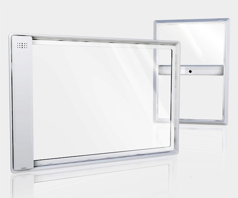
Tablet computers are definitely the wave of the future, and I am pretty sure we’ll see them evolve quickly over the next several years. This concept tablet PC is a gorgeous rendering of what might be possible in the future of the tablet.


The Iris Tablet PC is the work of designers Liu-Wei, Yao Kai-Chi, Hong Ruei-Hong & Cheng Ya-Fang. With a transparent body and OLED screen, the Iris is more a tool of augmented reality than a true tablet computer.


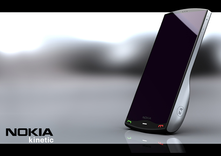
Nokia Kinetic concept phone with flexible display


Here’s a concept device from Nokia called the Kinetic. You use it by bending and twisting. It is not a touchscreen. Nokia Kinetic is a landscape device with two working applications, Music and Pictures.The Nokia Kinetic by Nokia Research division works by bending and twisting the device in each corner in order to register input.For example bending in the device towards you will open the application This new technology is very beneficial for those who live in cold environments because gloves don’t work well with touchscreens. Nokia Kinetic device feels like a step into the future, with a real OLED display Unfortunately, CNET reports that its strictly in the prototype phase, and may never become an actual product that’s for sale
.

Below is a video demo of the Nokia Kinetic and how it works.


Plasma antennas

The future of high-frequency, high-speed wireless communications could very well be plasma antennas capable of transmitting focused radio waves that would quickly dissipate using conventional antennas


The different states of matter generally found on earth are solid, liquid and gas. Sir William Crookes, an English physicist, identified a fourth state of matter, now called plasma, in 1879. Plasma is by far the most common form of matter. Plasma in the stars and in the tenuous space between them makes up over 99 per cent of the visible universe and perhaps most of what is not visible. Important to antenna technology, plasmas are conductive assemblies of charged and neutral particles and fields that exhibit collective effects. Plasmas carry electrical currents and generate magnetic fields. A plasma antenna is a type of antenna in which the metal-conducting elements of a conventional antenna are replaced by plasma. These are radio frequency antennas that employ plasma as the guiding medium for electromagnetic radiation. The plasma antennas are essentially a cluster of thousands of diodes on a silicon chip that produces a tiny cloud of electrons when charged. These tiny, dense clouds can reflect high-frequency waves like mirrors, focusing the beams by selectively activating particular diodes. The ‘beam-forming’ capability could allow ultra-fast transmission of high data loads—like those needed to seamlessly stream a TV show to an untethered tablet—creating an attractive option for the next generation of supercharged wireless transmitters. Many types of plasma antennas can be constructed, including dipole, loop and reflector antennas. Plasma antennas are interpreted as various devices in which plasma with electric conductivity serves as an emitting element. In gas plasma antenna the concept is to use plasma discharge tubes as the antenna elements. When the tubes are energised, these turn into conductors, and can transmit and receive radio signals. When de-energised, these revert to non-conducting elements and do not reflect probing radio signals. The fact that the emitting element is formed over the interval needed for the emission of an electromagnetic pulse is an important advantage of plasma antennas. In the passive state (in the absence of plasma in the discharge tube), such a device does not exhibit electric conductivity. A plasma stream flowing from a jet into the ambient space, the plasma trace of a body moving at an ultrasonic velocity in the atmosphere, and alternative plasma objects have been studied as possible antenna elements. Solid-state plasma antenna uses beamforming technology and the same manufacturing process that is currently used for silicon chips. That makes it small enough to fit into smartphones. Higher frequencies mean shorter wavelengths and hence smaller antennas...............


About HTML5?

So What’s New in HTML 5?

Well if you look at the HTML5 websites and applications you may feel that it is more of a programming language, but the truth is that it’s the same old HTML with some new markup tags and attributes, which make web designing easier than ever before. It’s backward compatible with HTML4 and thus you need not learn it from scratch. The new semantic tags, web page segmentation, the new link types, improved Media Handling with and tags are just a few important new features that we will discuss in this article, that are sure to affect your SEO strategies.....

Acoustic diode allows sound waves to only travel in one direction


When it comes to the sound-proofing of buildings, most people likely think of using materials that simply absorb the sound waves in a noisy room, so they can't proceed into a neighboring quiet room. Researchers at the California Institute of Technology (Caltech), however, are taking a different approach. They have created something known as an acoustic diode, that only allows sound traveling through it to go in one direction. If incorporated into building materials, such diodes would let sound travel from the quiet room to the noisy one, but would simply block noise transmission in the opposite direction.


The acoustic diode works much like a traditional electrical diode, which lets electrical currents pass in one direction, but keeps them from traveling back. In this case, sound waves are taking the place of electrical currents.

Researchers create hydrogen from ethanol using solar energy


Hydrogen is the most abundant element in the universe and its presence on our planet isnt limited. However, one problem with hydrogen is that it is not found in its pure form on the earth, which means that it has to be extracted from sources such as methane and water, both of which require a lot of energy. A team of researchers at Spains Universitat Politcnica de Catalunya, Scotlands University of Aberdeen and New Zealands University of Auckland have now created a process, using which hydrogen can be produced from renewable ethanol using sunlight.......

Green Transformer – Solar-powered algae refinery floats on water

Displayed at Seoul International Design Competition 2010, the Green Transformer is a concept algae refinery that is supposed to extract valuable bio-oil from algae in pools and ponds. The entirely solar-powered, floating processing plant makes use of a certain chemical additive during the suction to produce biodiesel for automobile and vessels. Moreover, the mechanism helps in removing pollutants from our water bodies.


As you can see in the above image, the Green Transformer folds itself and the solar panels as well when it is not in use. Where the fan-like solar canopy shelters the algae under it, an oil tanks at its center collects oil for future use.


Mini Machine Brings 3D Printing Home


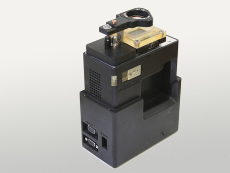
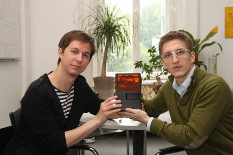
Three-dimensional printers are among the coolest futuristic technology already in use today, but they can be prohibitively expensive and very large. For those unfamiliar with the process of 3D printing, it involves a machine that lays down one layer of synthetic resin at a time while an intense beam of light hardens each layer in turn. The process allows precise shapes to be formed without casting or the need for large manufacturing setups. A team of Viennese researchers have come up with an additive manufacturing printer that is so small and affordable it could actually make the act of printing things we need an everyday action in ordinary homes


The machine is no bigger than a milk carton and weighs around three pounds, which is a huge reduction from the fridge-sized machines of 3D printing’s early years. At a cost of just €1200 (around $1700), it is remarkably affordable as well. The biggest advantage of 3D printers is that they can produce objects on demand, making it possible to create difficult-to-obtain spare parts without hassle. They also make it simple to produce toys, jewelry or other objects that you dream up but have no way of putting into mass production. The team from Technische Universitat Wien says that they will continue to make the machine smaller and smaller – so one day you might be able to whip a 3D printer out of your pocket to make last-minute gifts on the way to a party

World record 26 terabits per second data transmission achieved


With video content consuming ever more bandwidth, the need for faster data transmission rates has never been greater. Now a team of scientists at Germany's Karlsruhe Institute of Technology (KIT) are claiming a world record in data transmission with the successful encoding of data at a rate of 26 terabits per second on a single laser beam and transmitting it over a distance of 50 km (31 miles). The scientists claim this is the largest data volume ever transported on a laser beam and enables the transmission of 700 DVD's worth of content in just one second.


With no electronic processing methods available for a data rate of 26 terabits per second, the team developed a new opto-electric data decoding process. This process relies on purely optical calculations to break down the initial high data rate into smaller bit rates that can then be processed electrically. The record-breaking data encoding also employed the orthogonal frequency division multiplexing (OFDM) scheme based on Fast Fourier Transformation (FFT) mathematical routines that is commonly used in mobile communications networks including digital TV and audio broadcasts.


Because energy is required for the laser and a few process steps only, the team says the new method is not only extremely fast, but also very energy efficient.


"Our result shows that physical limits are not yet exceeded even at extremely high data rates," says Professor Jürg Leuthold, who led the KIT experiment. "A few years ago, data rates of 26 terabits per second were deemed utopian even for systems with many lasers and there would not have been any applications. With 26 terabits per second, it would have been possible to transmit up to 400 million telephone calls at the same time. Nobody needed this at that time. Today, the situation is different."


The latest breakthrough follows on from the previous high-speed data transmission record set by the KIT scientists in 2010, when they successfully exceeded the data rate of 10 terabits (or 10,000 billion bits) per second.


The KIT experiment involved companies and scientists from all over Europe, including members of the staff of Agilent and Micram Deutschland, Time-Bandwidth Switzerland, Finisar Israel, and the University of Southampton in Great Britain. The experiment is detailed in the journal Nature Photonics.

New 3D transistor design to speed up your PC


Intel announced on 4/5/11 Wednesday that it had again found a way to make computer chips that could process information more quickly and with less power in less space.

The transistors on computer chips — whether for PCs or smartphones — have been designed in essentially the same way since 1959 when Robert Noyce, Intel's co-founder, and Jack Kilby of Texas Instruments independently invented the first integrated circuits that became the basic building block of electronic devices in the information age.

These early transistors were built on a flat surface. But Intel is now building up. When the space between the billions of tiny electronic switches on the flat surface of a computer chip is measured in the width of just dozens of atoms, designers needed the third dimension to find more room.

The company has already begun making its microprocessors using a new 3D transistor design, called a Finfet (for fin field-effect transistor), which is based around a remarkably small pillar , or fin, of silicon that rises above the surface of the chip. Intel , based in Santa Clara, California , plans to enter general production based on the new technology some time later this year.

Although the company did not give technical details about its new process in its Wednesday announcement, it said that it expected to be able to make chips that run as much as 37% faster in low-voltage applications and it would be able to cut power consumption as much as 50%.

Intel currently uses a photolithographic process to make a chip, in which the smallest feature on the chip is just 32 nanometers, a level of microscopic manufacture that was reached in 2009. (By comparison a human red blood cell is 7,500 nanometers in width and a strand of DNA is 2.5 nanometers .) "Intel is on track for 22-nanometer manufacturing later this year," said Mark T Bohr, an Intel senior fellow and the scientist who has overseen the effort to develop the next generation of smaller transistors.

The company's engineers said that they now felt confident that they would be able to solve the challenges of making chips through at least the 10-nanometer generation, which is likely to happen in 2015.

Related Posts Plugin for WordPress, Blogger...